Logistics of a Hardware Implant
During the recent SaciCon I gave a short insight into to the magic Chinese hardware implant covered by Bloomberg from a hardware hacker’ s perspective. In summary I described it as a hardware hacker’s wet dream, simply due to size, effort and the feature set described by Bloomberg. Obviously I didn’t want to discuss any conspiracies, so I just stuck to the technical aspects. As an addition, I decided to cover the practical logistics of a hardware implant in a short post here. Thus, here an introduction into backdooring an Arduino Uno.
An Imaginary Implant and a Few Thoughts
For this post we’ll be dealing with an imaginary implant, it does everything we want, the way we want and when we want. It is not limited in power and size (it’s just as small as we need it). This also implies that our implant would have to offer some kind of connectivity to the outside (RF) or standalone capabilities. The only constraint we’ll have to cover is the actual connectivity into the existing circuit. Thus it needs enough connections / pins. Also every implant will need to be connected to a power source (VCC and GND).
Obviously any kind of implant on an Arduino can easily be detected as the base circuit contains less than 50 parts. Still we will aim at blending the implants into the overall design.
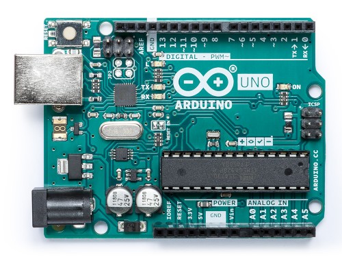
The Arduino Uno
The Arduino Uno is a low cost dev board used by many. The design is OpenHardware and fully documented on the Arduino Webpage.
 |
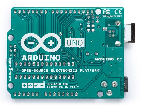 |
Why is the bottom flipped? Well, we’ll be looking at traces on the PCB, as such the picture is rotated to offer the same perspective as the layout below.
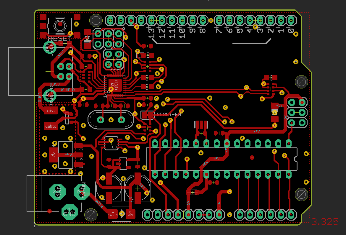
The layout looks like this
 |
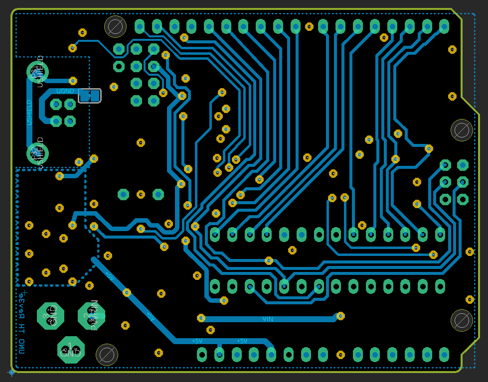 |
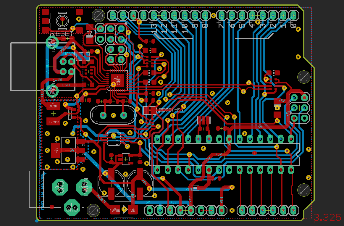
These are simple screenshots from eagle.
All red lines are copper routed on the top of the PCB, blue is from the bottom. The yellow circles are vias and connect the bottom and the top layer. The green areas are exposed pads / vias / parts of footprints where actual components are placed and soldered onto.
Together the layers look like this
The Arduino Uno is powered by an ATmega328P in a DIP/DIL 28 package running at 16MHz. It can be powered via USB or an extra power socket. Using a DCDC converter it can be run from up to 20V. As the ATmega328P does not support USB, the board also contains a ATmega16U2 which is programmed as an ISP adapter, or rather a USB to serial converter.
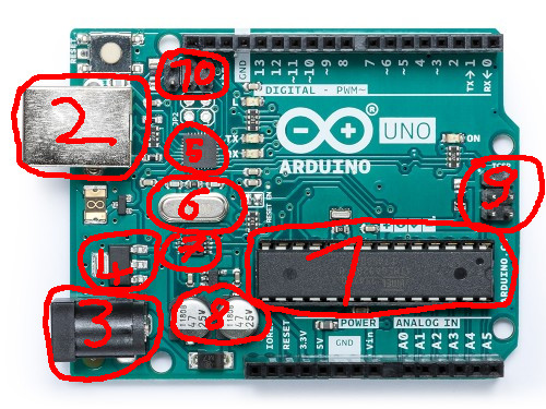
- ATmega328P
- USB B socket
- Power socket
- DCDC converter
- ATmega16U2
- Crystal for ATmega16U2
- Resistor Network
- Capacitors
- Programming header for ATmega328P
- Programming header for ATmega16U2
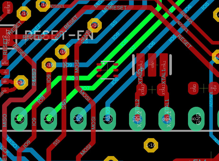
Implant #1
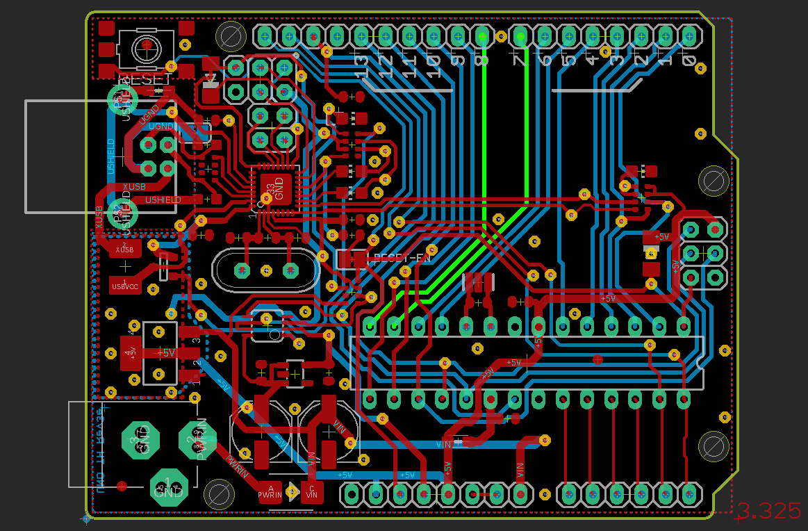
Our first implant will be aimed at intercepting two I/O pins. For this example we’ll choose the pins 7 and 8, which are highlighted in the next image
Intercepting means we want our implant to be placed between the main controller and the peripheral or for our Arduino the header. As such it will have to placed close to or actually within the highlighted lines. While the lines are routed on the bottom side of the PCB all parts are placed on top, so our implant will have to go on the opposite side than the lines are.
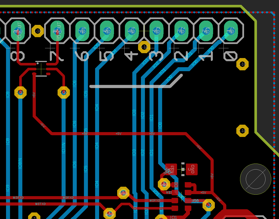
To be able to connect the lines from the bottom to the chip on the top, two vias had to be added. As such the lines IO8IN and IO7IN terminate in our implant, which is connected to the headers by IO8OUT and IO7OUT. To power the chip, we also had to add a connection to the next +5V line. Sadly the position of the implant is really obvious, as it’s placed somewhere where there shouldn’t be any parts at all.
Second Try
We’ll now try to place our implant closer to the main controller, thus hiding it in plain sight. While we have enough space for the chip itself, we will yet again have to do a fair amount of shifting lines to be able to also add the vias.
As we can see, it’s not impossible but does yet again require some rerouting and working at a different scale. By default the data lines on the Arduino Uno are 0.4064mm wide and the vias have a diameter of 0.6069mm. To be able to squeeze the implant, vias and lines in there we had to reduce the width down to 0.2mm and the drill diameter down to 0.3mm. While these sizes are typical for modern PCBs (I already had to change the width to be able to connect to the chosen chip package in the first example), the smaller a PCB is, the harder it is to actually add things in between.
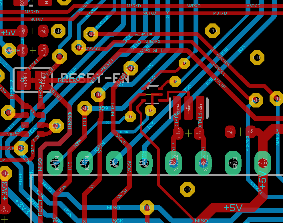
I guess you get the idea how it’s done.
Implant #2
Let’s say we now want to be able to access both lines from the ATmega328P and also the SPI interface of the ATmega16u2, which are highlighted in the next image.
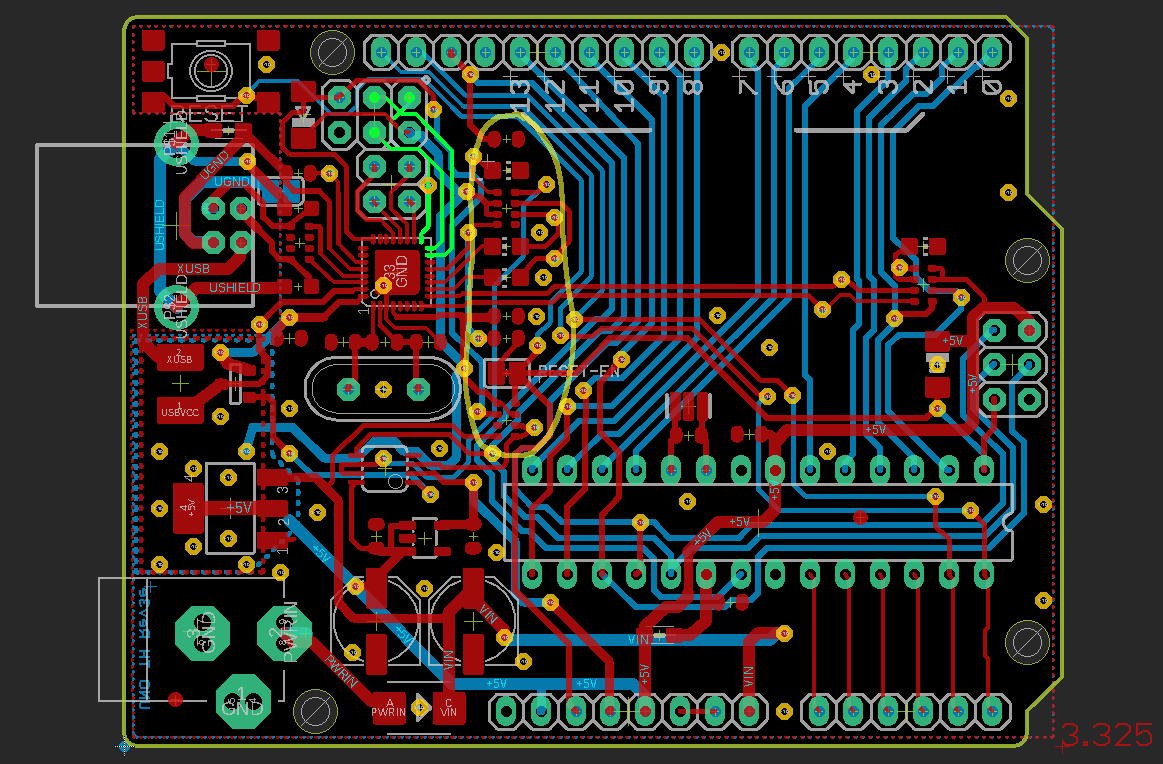
As the SPI interface is basically the programming interface for the ATmega16u2’s flash memory, it is obviously very interesting to have access to. Sadly we have a large block of parts in the way (marked by the yellow line). To be able to access both lines from the ATmega328P and the ATmega16u2 a rather big redesign of the PCB will be necessary. Due to all IO lines for the headers being routed along the bottom side, it will probably be necessary to move some of the parts.
We would also have to change the chip package, as the our current one only has 6 pins.
A More Complex PCB
The following Image shows the layout of Great Scott Gadget’s HackRF One. As we can see, it is designed by far tighter and in smaller dimensions than the Arduino Uno.
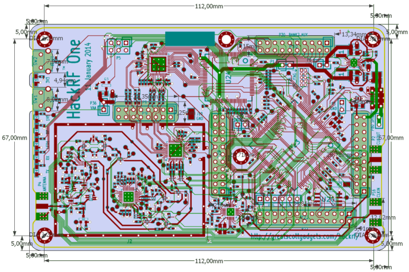
Source: Official HackRF Repo in GitHub
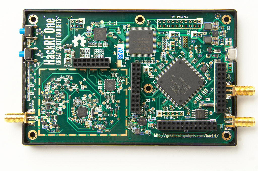
It should be obvious that while hiding something in the “chaos” of parts and data lines becomes easier, it is also by far more work to shift lines and parts to create a perfect placement for the implant. It also has to be noted that some lines are timing critical (and have to be just as long as the line next to it) or carry differential signals (and must stay parallel and in a certain distance to the next line). This makes it next to impossible to inject into these lines and adds a certain challenge to rerouting.
Buses
Up to here we’ve always aimed at connecting to individual data lines. In more complex environments components are connected via buses. The probably best known bus nowadays is USB, the Universal Serial Bus, which enables connecting various devices to a computer and when using a Hub, even connecting multiple devices to the same port. The basis of these buses is always some kind of address scheme, thus giving each device an individual ID so it can be specifically addressed. Above this most buses have some form of master / slave hierarchy. Where the master has control and either actively polls the slaves to see whether they have something they’d like to do or the slave has a way to raise it’s hand.
Attacking a bus can be a very effective way to get deep system access in many different environments. For the USB example an implant might be able to emulate many different client devices and attack the host / master. For some inspiration have a look at TURNIPSCHOOL. In cars for example one might add an extra node to the central CAN bus (or one of the 2..3..4 separate buses in each car) and thus gain access to most components in the vehicle.
For a PC one might aim at attacking something like the SMBus (System Management Bus). This was recently PoCed by Kudelski Security and described in a blog post here. Sadly SMBus isn’t a highspeed interface and productively messing with the system isn’t trivial. Alternativly one can have a closer look at PCI/PCIe as done by Ulf Frisk in his PCILeech project. Here it is important to understand that even a PCIe x1 interfaces uses 18 individual pins, which results in needing a rather large package for the implant. In addition one also has to list the firewire attacks as performed by the inception tool, which can be used as inspiration for further bus attacks.
The downside of “being part of a bus” is obviously direct visibility. I.e. When actively talking USB, the device will be enumerated by the host OS, the same when being a typical PCIe card in the system.
All of the examples above could be packed into dedicated chip and placed as an hardware implant, of course only after creating space to place it.
It is also important to note that systems usually have multiple buses for multiple purposes connecting only a specific components with each other. So one might end up having to access multiple buses.
Summary
While adding a hardware implant to a system is surely not impossible, it will force a partial redesign of the target circuit. This implies a significant amount of knowledge for identifying the best spot for injecting the implant and a fair amount of capacities for performing the actual redesign. So while the attack as described by Bloomberg is surely not impossible, it does require a fair amount of preparation and will result in changes easily seen by an external quality assurance process. (I guess the question here is if assurance is only performed on site in the factory or if there are random checks after leaving the factory.) Although modern mainboards are multi-layer-PCBs (layers in between that can’t be seen from the outside), the use of X-Ray is a typical approach when performing tests and should expose the changes performed while adding a physical implant.
:)
Ironically the best spots for implants are usually taken by the system components and the Arduino Uno is a perfect example for a demonstration of this.
Below we have two images of different versions of the Arduino Uno. The original and the Wattuino Uno.
|
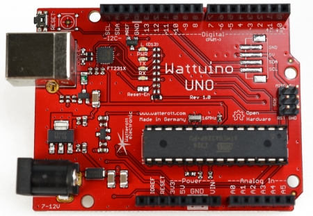 |
Both are based on the same original design and though using different packages (i.e. the two capacitors next to the power socket), both boards have the same functionality. The most significant difference is the USB interface. While the original, as described above, uses a programmable ATmega16u2 the Wattuino uses a FTDI FT231X USB USB to serial interface. When talking about attacking the core controller of the Arduino (the ATmega328P) the programming interface is a very nice target. Thus being able to reprogramm the chip that performs the programming of the converter is quite a nice approach. Thinking about this, it can often be more stealthy and easier to replace a component in the original design, rather than adding something. As such one might look at the original design as a backdoorable version of the Wattuino Uno :)